(China (Mainland))


Product Summary
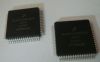
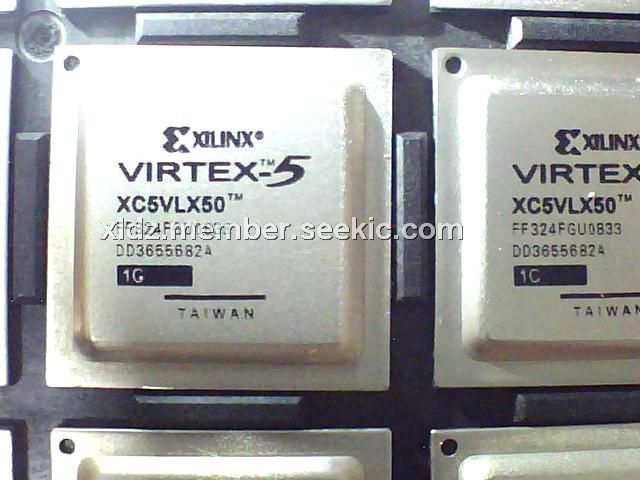
The XC5VLX50-1FF324C is an FPGA. The XC5VLX50-1FF324C is available in -3, -2, -1 speed grades, with -3 having the highest performance. The XC5VLX50-1FF324C contains many hard-IP system level blocks, including powerful 36-Kbit block RAM/FIFOs, second generation 25 x 18 DSP slices, SelectIO technology with built-in digitally-controlled impedance, ChipSync source-synchronous interface blocks, system monitor functionality, enhanced clock management tiles with integrated DCM (Digital Clock Managers) and phase-locked-loop (PLL) clock generators, and advanced configuration options.
Parametrics
XC5VLX50-1FF324C absolute maximum ratings: (1)Internal supply voltage relative to GND:–0.5 to 1.1 V; (2)Auxiliary supply voltage relative to GND:–0.5V to 3.0V; (3)Output drivers supply voltage relative to GND:–0.5V to 3.75V; (4)Key memory battery backup supply:–0.5V to 4.05V; (5)Input reference voltage:–0.5V to 3.75V; (6)3.3V I/O input voltage relative to GND(user and dedicated I/Os):–0.75V to 4.05V; (7)3.3V I/O input voltage relative to GND (restricted to maximum of 100 user I/Os):–0.95V to 4.4V (Commercial Temperature),-0.85V to 4.3V(Industrial Temperature); (8)2.5V or below I/O input voltage relative to GND (user and dedicated I/Os):–0.75V to VCCO + 0.5V; (9)Current applied to an I/O pin, powered or unpowered:±100 mA; (10)Total current applied to all I/O pins, powered or unpowered:±100 mA; (11)Voltage applied to 3-state 3.3V output(user and dedicated I/Os):–0.75V to 4.05V; (12)Voltage applied to 3-state 2.5V or below output (user and dedicated I/Os):–0.75V to VCCO + 0.5V; (13)Storage temperature (ambient):–65℃ to 150℃; (14)Maximum soldering temperature:+220℃; (15)Maximum junction temperature:+125℃.
Features
XC5VLX50-1FF324C features: (1)In-System Programmable PROMs for Configuration of Xilinx FPGAs; (2)Low-Power Advanced CMOS NOR FLASH Process; (3)Endurance of 20,000 Program/Erase Cycles; (4)Operation over Full Industrial Temperature Range(–40℃ to +85℃); (5)IEEE Standard 1149.1/1532 Boundary-Scan (JTAG) Support for Programming, Prototyping, and Testing; (6)JTAG Command Initiation of Standard FPGA Configuration; (7)Cascadable for Storing Longer or Multiple Bitstreams; (8)Dedicated Boundary-Scan (JTAG) I/O Power Supply(VCCJ); (9)I/O Pins Compatible with Voltage Levels Ranging From1.5V to 3.3V; (10)Design Support Using the Xilinx Alliance ISE and Foundation ISE Series Software Packages.
Diagrams
| Image | Part No | Mfg | Description |  |
Pricing (USD) |
Quantity | ||||||
|---|---|---|---|---|---|---|---|---|---|---|---|---|
 |
 XC5VLX50-1FF324C |
|
IC FPGA VIRTEX-5 50K 324FBGA |
Data Sheet |
|
|
||||||
| Image | Part No | Mfg | Description | |
Pricing (USD) |
Quantity | ||||||
 |
XC5VFX100T-1FF1136I |
|
IC FPGA VIRTEX-5FXT 1136FFBGA |
Data Sheet |
|
|
||||||
|
XC5VFX100T-1FF1738I |
|
IC FPGA VIRTEX-5FXT 1738FFBGA |
Data Sheet |
|
|
||||||
|
XC5VFX100T-1FFG1136C |
|
IC FPGA VIRTEX 5 100K 1136FFGBGA |
Data Sheet |
|
|
||||||
|
XC5VFX100T-1FFG1136I |
|
IC FPGA VIRTEX 5 100K 1136FFGBGA |
Data Sheet |
|
|
||||||
|
XC5VFX100T-1FFG1738C |
|
IC FPGA VIRTEX 5 100K 1738FFGBGA |
Data Sheet |
|
|
||||||
|
XC5VFX100T-1FFG1738I |
|
IC FPGA VIRTEX 5 100K 1738FFGBGA |
Data Sheet |
|
|
||||||